Tapeout
Tape Out is the hand over point from the SoC design flow to the physical device fabrication flow. It is usually the point where the design is past from the designers to the wafer production facility. There may be an intermediate step if the design is to be combined with others as part of a Multi-Part Wafer (MPW) service.
One of the key aspects is translating the final design into mask sets used in the key part of the fabrication process, the photo-lithograpy steps that pattern the wafer to build up the features that make the functional devices. The skills with Tape Out involve using Computer Aided Design software to inspect and qualify the many layers of circuit/device design which are made into masks. As well as checking before submission that non of the wafer foundry rules have been violated the work may need to respond to issues identified in checks at the foundry that could cause potential problems in manufacturing the design.
Projects Using This Design Flow
megaSoC
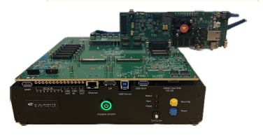
Reference Design Comparison Table
This table will let you compare this reference design with others on SoC Labs| Title | megaSoC | milliSoC |
|---|---|---|
| Class | Complex | Mid-range |
| Reference Design | MegaSoC | TSRI/SoC Labs |
| Staffing | Academic team | Academic + dedicated post doc |
| Time Scales | 6 months to 1 year | 1+ years |
| Model Forms | Trial of processing element | |
| Tape Out / Package and Board Costs | >£50k | £25k-£50k |
| Processor(s) | A53 | M55/U55 |
| Processor(s) (speed) | > 800 Mhz | 250-800Mhz |
| Data Rates / On Chip Comms | <2.5 Gbps | 10-80 Gbps |
| Data Rates / Off Chip Comms | <50 Mbps | 0.1-0.8 Gbps |
| On Chip Memory Requirements | 32KB to multiple MB | 2MB+ |
| Virtual Prototype Environment | HAPS | MPS3 |
| Tape Out Node | 28nm | 28nm |
Related Projects and Workflows
This section details the following: the core reference design, the initial project that led to the definition of the reference design, and any additional projects that extend the reference design for new or additional applications. It also defines the related example workflows for the front end Architectural and Behavioural design stages, and the back end Logical and Physical design stages. Front end Behavioural design are usually accomplished with FPGA environments and tool chains, back end Physical design requires technology specific design rules and EDA tool suites.
Related Project Milestones
| Project | Name | Target Date | Completed Date | Description |
|---|---|---|---|---|
| Project Milestone Overview example | Tape Out (82) |
Test add |