Universal Verification Methodology
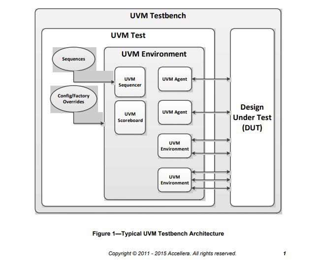
The Universal Verification Methodology (UVM) is a standard to create a modular reusable generic verification environment. It aims to reduce the effort of reusing IP by making it easier to reuse verification components associated with the IP.
UVM provides an architectural framework and class libraries for establishing verification environments for a Design Under Test (DUT). A Testbench is a flexible way to create a structured approach to verify IP. It instantiates the IP as a DUT and Test which contains a set of configured verification components and applies sequences of transactions to the DUT. The verification environment for a SoC will contain a hierarchy of Environment components with typically one per IP component. An Agent within the Environment manages a stimulus flow of transaction that are applied to the DUT. Within the Agent transactions from a Sequencer are past to a Driver that converts the transaction-level stimuli into pin-level stimuli and probe the DUT interface with drive signals. A Monitor captures the output of the DUT and converts the pin-level activity to transactions which are passed into the verification environment for analysis. A Scoreboard uses a reference model to check the behavior of DUT comparing the actual and expected transactions flowing through the various Agents.
UVM provides a level of abstraction to the verification process using Transaction-Level Modeling (TLM) and also allows for mixed-language verification environments. While the UVM provides an interoperable standard for creating components within a verification environment there are still different implementation choices which need to be considered at this stage of the SoC project.
Projects Using This Design Flow
megaSoC
Reference Design Comparison Table
This table will let you compare this reference design with others on SoC Labs| Title | megaSoC | milliSoC |
|---|---|---|
| Class | Complex | Mid-range |
| Reference Design | MegaSoC | TSRI/SoC Labs |
| Staffing | Academic team | Academic + dedicated post doc |
| Time Scales | 6 months to 1 year | 1+ years |
| Model Forms | Trial of processing element | |
| Tape Out / Package and Board Costs | >£50k | £25k-£50k |
| Processor(s) | A53 | M55/U55 |
| Processor(s) (speed) | > 800 Mhz | 250-800Mhz |
| Data Rates / On Chip Comms | <2.5 Gbps | 10-80 Gbps |
| Data Rates / Off Chip Comms | <50 Mbps | 0.1-0.8 Gbps |
| On Chip Memory Requirements | 32KB to multiple MB | 2MB+ |
| Virtual Prototype Environment | HAPS | MPS3 |
| Tape Out Node | 28nm | 28nm |
Related Projects and Workflows
This section details the following: the core reference design, the initial project that led to the definition of the reference design, and any additional projects that extend the reference design for new or additional applications. It also defines the related example workflows for the front end Architectural and Behavioural design stages, and the back end Logical and Physical design stages. Front end Behavioural design are usually accomplished with FPGA environments and tool chains, back end Physical design requires technology specific design rules and EDA tool suites.

Related Project Milestones
| Project | Name | Target Date | Completed Date | Description |
|---|---|---|---|---|
| Project Milestone Overview example | Universal Verification Methodology (119) |
Test |
Explore This Design Flow