Architectural Design
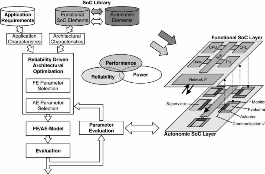
The concept of reusable design patterns is familiar to many disciplines. At SoC Labs we are interested in reusable design patterns incorporating Arm based components with parts that are unique to your specific research challenge.
Arm itself uses the term Architecture for defining the processor instruction set, programmers' model and memory model, but not implementation details such as cache sizes. Your SoC design is likely a selection and configuration of Arm IP to define the main architecture with specific blocks either developed uniquely or existing third party blocks modified or arranged in a novel way.
The first step is determining the information needed to begin architectural design. Often described as a Specification it should include a list of the proposed uses, specific algorithms or calculations that are to be implemented, time critical operations, etc.
Based on the Specification the next step is to select design components or IP Selection.
At this high level stage of the design process their is less interested in ultimate use of area, power or performance. The interest is in relative observations for different architectural design decisions. The tools available usually rely on static information for area, power and performance that is adjusted/calculated from available configuration database as different architectural designs are evaluated. This can be high level selection such as which processor to use or more fine grained in terms of data paths, cache sizes, etc.
Projects Using This Design Flow
megaSoC
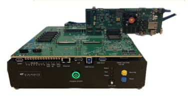
Reference Design Comparison Table
This table will let you compare this reference design with others on SoC Labs| Title | megaSoC | milliSoC |
|---|---|---|
| Class | Complex | Mid-range |
| Reference Design | MegaSoC | TSRI/SoC Labs |
| Staffing | Academic team | Academic + dedicated post doc |
| Time Scales | 6 months to 1 year | 1+ years |
| Model Forms | Trial of processing element | |
| Tape Out / Package and Board Costs | >£50k | £25k-£50k |
| Processor(s) | A53 | M55/U55 |
| Processor(s) (speed) | > 800 Mhz | 250-800Mhz |
| Data Rates / On Chip Comms | <2.5 Gbps | 10-80 Gbps |
| Data Rates / Off Chip Comms | <50 Mbps | 0.1-0.8 Gbps |
| On Chip Memory Requirements | 32KB to multiple MB | 2MB+ |
| Virtual Prototype Environment | HAPS | MPS3 |
| Tape Out Node | 28nm | 28nm |
Related Projects and Workflows
This section details the following: the core reference design, the initial project that led to the definition of the reference design, and any additional projects that extend the reference design for new or additional applications. It also defines the related example workflows for the front end Architectural and Behavioural design stages, and the back end Logical and Physical design stages. Front end Behavioural design are usually accomplished with FPGA environments and tool chains, back end Physical design requires technology specific design rules and EDA tool suites.
Related Project Milestones
| Project | Name | Target Date | Completed Date | Description |
|---|---|---|---|---|
| Project Milestone Overview example | Architectural Design (92) |
Explore This Design Flow