RTL Design
Takes an Architectural Model and creates a full behavioural description of a system that can be run in simulators or transformed into a technology independent register-transfer level (RTL) description.
System on Chip (SoC) designs often integrate digital and analogue circuits and these require different models and methods of simulation and verification.
In the digital domain Transaction-Level Modelling (TLM) can create a behavioural description of a system with enough detail to allow verification of the design by simulation but abstracting the designer from many detailed implementation concerns. TLM can be undertaken at different levels of abstraction. At the highest level of abstraction untimed models consist of computation objects that send and receive abstract data via communications objects. In SystemC the computation objects (Module/Process) interact via communications objects (Channels/Ports). Further stages of refinement reduce the abstraction and add more implementation detail, for example specific bus protocols can be added in either cycle approximate models using simplified estimated times or cycle accurate models where explicit timing, pin and even wire details are added. An implementation level model is one where components are modelled at register-transfer level.
While the digital domain operates in pure Boolean behaviour the analogue domain can have continuous-time, non-linear behaviours. Behavioural models for the analogue domain use forms of mathematical approximation, linear or non-linear regression, neural networks, etc. to define relations between inputs and outputs of the circuit and can have long simulation times.
Projects Using This Design Flow
megaSoC
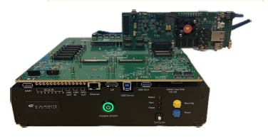
Reference Design Comparison Table
This table will let you compare this reference design with others on SoC Labs| Title | megaSoC | milliSoC |
|---|---|---|
| Class | Complex | Mid-range |
| Reference Design | MegaSoC | TSRI/SoC Labs |
| Staffing | Academic team | Academic + dedicated post doc |
| Time Scales | 6 months to 1 year | 1+ years |
| Model Forms | Trial of processing element | |
| Tape Out / Package and Board Costs | >£50k | £25k-£50k |
| Processor(s) | A53 | M55/U55 |
| Processor(s) (speed) | > 800 Mhz | 250-800Mhz |
| Data Rates / On Chip Comms | <2.5 Gbps | 10-80 Gbps |
| Data Rates / Off Chip Comms | <50 Mbps | 0.1-0.8 Gbps |
| On Chip Memory Requirements | 32KB to multiple MB | 2MB+ |
| Virtual Prototype Environment | HAPS | MPS3 |
| Tape Out Node | 28nm | 28nm |
Related Projects and Workflows
This section details the following: the core reference design, the initial project that led to the definition of the reference design, and any additional projects that extend the reference design for new or additional applications. It also defines the related example workflows for the front end Architectural and Behavioural design stages, and the back end Logical and Physical design stages. Front end Behavioural design are usually accomplished with FPGA environments and tool chains, back end Physical design requires technology specific design rules and EDA tool suites.
Related Project Milestones
| Project | Name | Target Date | Completed Date | Description |
|---|---|---|---|---|
| Project Milestone Overview example | Behavioural Design (98) |