Real-Time Edge AI SoC: High-Speed Low Complexity Reconfigurable-Scalable Architecture for Deep Neural Networks
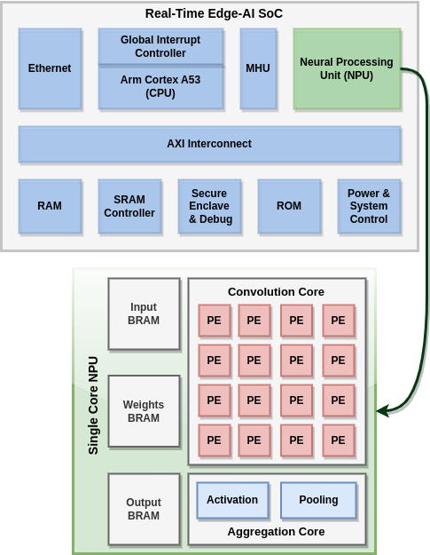
Modern Convolutional Neural Networks (CNNs) are known to be computationally and memory costly owing to the deep structure that is constantly growing. A reconfigurable design is crucial in tackling this difficulty since neural network requirements are always evolving. The suggested architecture is adaptable to the needs of the neural network. The suggested architecture is flexible enough to compute various networks with any size input image. System-on-Chip (SoC) development for this accelerator is required in order to provide a single-chip solution for CNN edge inference that incorporates preprocessing of the data and layerwise control over the inputs and outputs. The tight coupling between the accelerator and other components, such as memory interfaces and peripherals, is made possible by integrating our accelerator, also known as the NPU (Neural Processing Unit), into a SoC. This makes data movement more effective and lowers the latency, which enhances the overall performance of the deep learning tasks. Also the host processing system, such as a CPU or GPU, can be seamlessly integrated with the NPU as a result of a SoC.
Through this connection, it is possible to transfer computationally demanding Deep Learning (DL) activities to the accelerator, offloading the host CPU for other tasks and enhancing system efficiency. The advantage of future extension and upgrades is available with a SoC-based NPU. The SoC can be upgraded to include superior accelerator architectures or other hardware components to keep up with the developments in DL capabilities as algorithms and technology evolve. By using customized algorithms on CPU to fragment the image and a dedicated controller to keep track of the different scheduling tasks to be implemented on the NPU, this SoC will be able to handle a range of image sizes as inputs to the CNN, proving that it is an image-scalable and reconfigurable NPU-based SoC. Additionally, the SoC may increase its access to cloud resources with the aid of an Ethernet connector, allowing it to apply effective neural network preprocessing methods like network adaptation, post-training quantization and pruning for CNNs with billions of weights in a digital-twin setup.
Project Milestones
Do you want to view information on how to complete the work stage ""
or update the work stage for this project?
-
Design upgradtions of NPU
Target Date- Designing dedicated data paths for NPU's control logic, kernels and input activation ports with AXI-Lite and AXI-Stream.
- Adding DMA support to the NPU for real-time data transfers from the processor and DDR memory.
- Generation of ASIC memory macros with TSMC 40nm and TSMC 28nm for replacing the register based Block RAMs.
- Unit-level testing of NPU after interface-level integration and FPGA based testing for power and area estimates.
- Configure/Verify DMA350 and NIC400 with Socrates/CoCotb to substitute the AXI-DMA and AXI-Interconnect from the existing design.
-
Unit-level verification of NPU
Target Date -
FPGA prototyping of NPU; NPU integration with SoC
Target Date -
System-level verification of SoC
Target Date -
OS building and virtual boot ; ASIC synthesis and preroute gatesims
Target Date -
System-level prototyping on FPGA with OS; Backend Design
Target Date -
ASIC backend design complete; DRC checks and STA
Target Date -
Tapeout
Target Date
Associated Organisations
 Indian Institute of Technology Hyderabad (IITH)
 Amit Acharyya
Indian Institute of Technology Hyderabad (IITH)
Professor
Research area: VLSI systems resource-constrained applications, Low Power Design Techniques, Machine learning hardware design, Signal Processing Algorithm and VLSI Architectures, Digital Arithmetic, Biomedical Devices. AI/ML, Nanoscience & Technology
ORCID Profile
Discussion
John Darlington
30 May 2023 - 22:15
Use of CoreLink NIC-450
The CoreLink NIC-450 you have identified provides some Arm blocks such as QoS-400 and QVN-400 that support Quality of Service protocols for specific latency concerns and other capabilities to better manage different data flows.
You have identified data movement efficiency and latency as key issues to overall performance of your deep learning tasks. You also mention using the CPU to fragment the image. Do you see the Quality of Service as important to your design?
John Darlington
30 May 2023 - 08:56
Welcome and an exciting project
Thanks for joining the contest and this looks like an exciting project. We look forward to seeing it develop.
Add new comment
To post a comment on this article, please log in to your account. New users can create an account.