Fast-kNN: A hardware implementation of a k-Nearest-Neighbours classifier for accelerated inference

Project Motivation and Goals
The k-Nearest-Neighbours (kNN) algorithm is a popular Machine Learning technique that can be used for a variety of supervised classification tasks. In contrast to other machine learning algorithms which "encode" the knowledge gained from training data to a set of parameters, such as weights and biases, the parameter set of a kNN classifier consists of just labelled training examples. Classification of an unlabelled example takes place by calculating its Euclidean distance (or any other type of distance metric) from all the stored training examples. The label of the unknown example is determined by the majority of the labels of the k closest examples.
In contrast to other Machine Learning methods, kNN classification doesn't require an explicit training phase, which makes it a potential candidate for learning directly from the data captured by an embedded system. However, the computation of the distance metrics between a new unclassified example and the labelled examples stored as the classifier's parameter set acts as a bottleneck in the classification process, if it is implemented in software. Through the development of dedicated hardware for calculating the required distance metrics, it is possible to reduce inference time.
The goal of this project is to build a hardware implementation of a kNN classifier that can achieve reduced inference time when compared to a kNN classifier implemented fully in software, through the parallelisation of distance metric computations. The project has an educational purpose and it expected that by its completion, the contributors will have gone through the complete design cycle of a SoC.
Design Specification
The first step in defining the design specification for the accelerator was to determine the type of data that need to be processed by it. The Fashion-MNIST dataset has been selected as the primary data source. Therefore, the accelerator should be able to handle grayscale image vectors with a size of 28 x 28 pixels. We assume that some of these images will be labelled (training set), while some of them won't (test set). The accelerator should help with computing the distance between all the labelled images and each unknown image in the unlabelled set.
Data to be processed: N 28 x 28 8-bit (grayscale) labelled image vectors and M unlabelled image vectors, stored in SRAM.
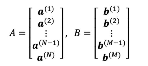
Image vectors a(i), b(j) have D elements, where D = 28 x 28 = 784. Each element is represented as an 8-bit unsigned integer value. If N = 200 and M = 50, the total storage requirements for matrices A and B are:
N x 785 + M x 784 = 200 x 785 + 50 x 784 = 196,200 bytes, which is approximately equal to 192 kB. It is assumed that one byte of storage is required for storing every label. This is the reason why the number of labelled examples N is multiplied by 785 and not 784.
We would like to compute the Squared Euclidean distance between each pair of vectors a(i), b(j). This computation is given by the sum of 3 dot products, as shown below:
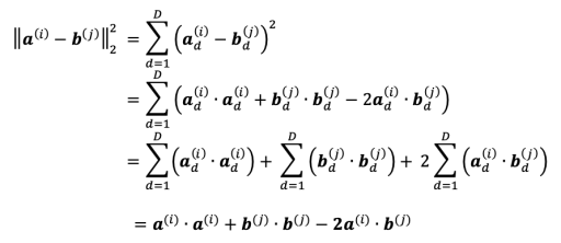
The self-dot products a(i)⋅a(i) and b(j)⋅b(j) can only be computed once and then reused for another computation.
Design Rationale
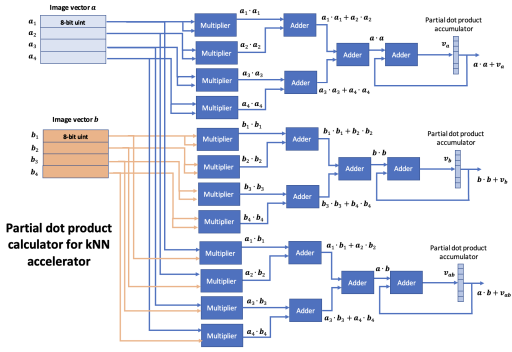
Because of the high dimensionality of the image vectors, it is proposed to divide the computation of the full dot products into a series of rounds. In each round, partial dot products are computed over a small number of elements. The partial dot products from each round, can be cached into an accumulator and reused in the next round to incrementally calculate the final full dot product. In the last round, the full-dot products are moved to SRAM.
In the case, where the full self-dot products are known, the modules of the accelerator that compute them should be turned off through configuration bits.
Accelerator Input Data Packet
Each round of computation can take place on 4 vector elements from each image vector. With 4 vector elements per round, the complete computation is expected to be completed after 784 / 4 = 196 rounds. Each input packet for the accelerator wrapper is built from 32-bit words. Therefore, there is a need for (2 x 4 x 8) / 32 = 2 words per data packet.
Project Milestones
Do you want to view information on how to complete the work stage ""
or update the work stage for this project?
-
First abstract description of project goals
Target DateRough outline of the project's goals, hardware accelerator idea and motivation.
-
Architectural description and Familirisation with design tools
Target Date- Specify the number format used for the arithmetic operations of the accelerator (i.e. 8-bit unsigned integers for grayscale images).
- Select the distance metric used for kNN classification (i.e. Euclidean distances).
- Determine the type of building blocks (i.e. adders, multipliers) required to perform the arithmetic operations.
- Capture the architectural design in block diagram format, specifying the necessary inputs, outputs, registers and the overall data flow.
- Complete the lab exercises from the "Introduction to SoC design" course to gain familiarity with Xilinx Vivado.
-
Milestone #3
Target Date -
Milestone #4
Target Date -
Milestone #5
Target Date -
Milestone #6
Target Date
Associated Organisations
 University of Southampton
 Epifanios Baikas
University of Southampton
PhD Student
Research area: Machine Learning on Resource-Constrained Embedded Systems
Discussion
John Darlington
25 Jul 2023 - 12:58
Design Progress
As Daniel suggests, looking for the sweet spot where the SoC as a system is optimised both in data processing (calculations and their parallelism) and data movement (minimising the time where the bus is not utilised) is aiming to a point where you are able to run the calculations as fast as you can move the data.
As outlined the two aspects to consider;
1) The SoC integration issue (outside in)
2) The accelerator design (inside out)
Increasing the data processing capacity can be brute parallelism, just replication of processing blocks or data data specific optimisations, black pixels that are represented as zero which could reduce computation. Does a black pixel in the input image not add any contribution to the distance to all other class members? Holding data is changing less frequently (the unknown example) while you iterate data for say the members of a class?
Increasing utilisation of the system to move the data associated with processing. This is the SoC integration issue. How to maximise the data flowing across the bus into your accelerator. Looking at the asymmetry of data input to calculated outputs.
In this contest pathway, it is not about the ultimate design, it is about your journey in looking at optimisation strategies both in the utility of the SoC infrastructure and the application domain calculations. Perhaps when you have a next view of your design and the thoughts behind it you can share it?
Daniel Newbrook
30 May 2023 - 08:56
Optimisation of Parrallelism
Hi Fanis,
I've see you've added some update to the architectural design of your project. And at the moment are looking to take in 4 x 8 bit words at a time. One potentially good approach to seeing how you can work on these dot products in parallel would be to use the architecture you've chosen as a starting point (2 parallel calculations of a1, a2, b1, b2) and through simulation see where your current bottleneck are. If the bottleneck is your data processing and not your data fetching, you could try increasing the number of parallel branches until you reach a point where you are able to run the calculations as fast as you can fetch data.
Taking this iterative approach can give you a good view of how to optimise your design for the nanosoc. Also if you take your current design all the way through to synthesis, you can then estimate what footprint a single dot product branch takes up. And estimate how many branches you would be able to fit in the tape out
Daniel
David Mapstone
22 May 2023 - 15:44
Vector Element Input
Hi Fanis,
With the vector input, you say you can put 4 vector inputs per 32-bit transaction. Are these all going to be from the same image and buffer them, are they going to be 2 vectors from image A and 2 from image B or will it change depending on where you are in your calculation flow?
Thanks,
David M
John Darlington
19 May 2023 - 12:36
Patterns and how they help
Identifying both Data Patterns and Design Patterns can really help in the design phase. Look at how the data in structured in the calculations in relation to the labelled data set and unknown examples and how they interact and the implication on their storage in memory and flow across the SoC. That will help identify the Design Patterns for the IP blocks.
John Darlington
23 May 2023 - 22:33
In reply to Patterns and how they help by John D
Data Patterns
Does the Fashion-MNIST dataset provide any natural advantages for processing. For example does the background being black mean the value 0 represents the background?
John Darlington
19 May 2023 - 12:30
Architectural design phase
It is good to see you working through the Architectural design phase and building the conceptual understanding of the design and design space for potential alternative designs.
It is interesting to consider the flow of 32-bit words over the bus into the accelerator and how these are structured compared to the original view for the labelled and unknown examples. How you can sequence the calculations and any intermediate results you can hold. Unlike the example SHA-2 accelerator that needs data aggregated from 32-bit words before it can undertake calculation in this case you may be able to undertake calculation more efficiently.
John Darlington
09 May 2023 - 13:39
Design Flow help
David and Daniel have added some items in the https://soclabs.org/design-flow/soc-design-contest-2023-example-flow that have some helpful questions such as can we at this stage identify and 'system bottlenecks'. Do other design decisions such as say the use of the 'reference design' constrain our design space, eg. how much data can we flow through the accelerator, what memory constrains/organisation. What area are we looking to deploy? How many calculations can we undertake in parallel? We can start to lay out questions and answers as part of conceptual understanding of a design.
John Darlington
04 May 2023 - 09:39
How did you get on with your May 1st milestone?
Hi,
It would be great if you could let us know how you are getting on with your May 1st Milestone and if there is any help you need for planning the next milestones and support in terms of generic reference design technology or design flow environment help?
Epifanios Baikas
04 May 2023 - 13:43
In reply to How did you get on with your May 1st milestone? by John D
Hi, I've been having some…
Hi, I've been having some issues while trying to familiarise myself with the tools introduced by the labs of the Intro to SoC design course offered by Arm Education Media. The presented workflow introduces Xilinx Vivado and Arm Keil, both of which require a Windows environment (I think Vivado can also run on Linux). I am a Mac user and as a consequence I had trouble using the software. I have tried using the Soclabs servers, but the interface seems to become irresponsive sometimes. I have been told that this might be caused by a screensaver setting, but I still need to check.
John Darlington
09 May 2023 - 13:24
In reply to Hi, I've been having some… by epi_baikas
Hopefully the advice on the…
Hopefully the advice on the local server has got you past that problem. Hopefully you can move on to the process of design. The process of design, like the design itself, can benefit from re-use. Design is a conceptual process and we often re-use techniques such as top down decomposition or bottom up. We can iterate between them to build out understanding. We can arm ourselves with questions that help rationalise the conceptual design.
In this case we have a known approach, k-Nearest-Neighbours (kNN) algorithm, and you have started to decompose this (top down). You also need to consider how you will calculate distances (bottom up). What is needed for each calculation and how does the SoC deliver that to allow the calculations to efficiently be undertaken. What are the limitations that are imposed by the SoC system and how best do we translate the mathematical algorithm onto it.
In the example accelerator we show some custom logic for performing calculations. We have data moving across the bus of the SoC and into the accelerator and results coming back out. In your example how symmetric is the data needed versus the result and does that have any implications? What is the pattern of data flowing across the bus? Asking such questions helps develop our understanding of the design. Design is as much about generating questions as it is about generating answers.
Perhaps you can share how you are developing your conceptual understanding of the Architectural Design space?
John Darlington
04 Apr 2023 - 23:03
Milestone Planning
Hi,
It would be good to try and lay out your initial plans for Milestones. You might want to look at the steps in the generic design flows and allocate them to Milestones. You might also want to look at the SoC Design Contest 2023 example flow for some help.
John.
Add new comment
To post a comment on this article, please log in to your account. New users can create an account.