CoreLink CCI-400
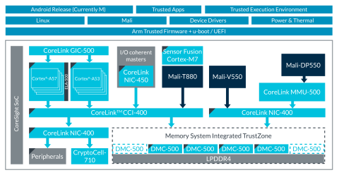
The Arm CoreLink CCI-400 Cache Coherent Interconnect provides full cache coherency between two clusters of multi-core CPUs. It enables big.LITTLE processing and I/O coherency for devices such as the Mali-T600 series GPU, and I/O masters like modem and USB. First released in 2011, CoreLink CCI-400 has been widely licensed and is today shipping in many millions of production devices.
Projects Using This Technology
megaSoC
Reference Design Comparison Table
This table will let you compare this reference design with others on SoC Labs| Title | megaSoC | milliSoC |
|---|---|---|
| Class | Complex | Mid-range |
| Reference Design | MegaSoC | TSRI/SoC Labs |
| Staffing | Academic team | Academic + dedicated post doc |
| Time Scales | 6 months to 1 year | 1+ years |
| Model Forms | Trial of processing element | |
| Tape Out / Package and Board Costs | >£50k | £25k-£50k |
| Processor(s) | A53 | M55/U55 |
| Processor(s) (speed) | > 800 Mhz | 250-800Mhz |
| Data Rates / On Chip Comms | <2.5 Gbps | 10-80 Gbps |
| Data Rates / Off Chip Comms | <50 Mbps | 0.1-0.8 Gbps |
| On Chip Memory Requirements | 32KB to multiple MB | 2MB+ |
| Virtual Prototype Environment | HAPS | MPS3 |
| Tape Out Node | 28nm | 28nm |
Related Projects and Workflows
This section details the following: the core reference design, the initial project that led to the definition of the reference design, and any additional projects that extend the reference design for new or additional applications. It also defines the related example workflows for the front end Architectural and Behavioural design stages, and the back end Logical and Physical design stages. Front end Behavioural design are usually accomplished with FPGA environments and tool chains, back end Physical design requires technology specific design rules and EDA tool suites.
Explore This Design Flow